The semiconductor industry is rapidly evolving, and with scaling technologies such as 90nm, 65nm, 45nm, and now sub-nanometer nodes, the design complexity of IC systems has increased dramatically. Modern industries rely heavily on EDA tools to simulate, test, optimize, and validate integrated circuits before fabrication. Among all tools, Cadence Virtuoso remains one of the most preferred platforms for analog, RF, and mixed-signal IC design workflows.
Students who explore VLSI Cadence Projects gain real-time experience with schematic design, layout development, design rule checking (DRC), layout-versus-schematic (LVS), parasitic extraction (PEX), mixed-signal simulation, and performance tuning.
Whether the goal is research, internship qualification, or placement preparation, working on realistic VLSI Cadence Projects gives final-year engineering students the practical exposure needed to advance in semiconductor careers.
The world of semiconductor design is evolving faster than ever, and with the growth of smart electronics, AI-enabled systems, tool devices, EV technology, and high-speed processors, the demand for advanced VLSI engineers is skyrocketing. At the heart of this technological evolution lies Cadence Virtuoso, one of the most widely used industry tools for analog, RF, and mixed-signal IC design.
Engineering students, researchers, and chip design aspirants who work on VLSI Cadence Projects gain hands-on experience in layout design, simulation, transistor modeling, and fabrication-aware circuit development. These project topics prepare learners for careers at global semiconductor companies such as Intel, Qualcomm, NVIDIA, Texas Instruments, TSMC, ARM, Samsung Semiconductor, and Synopsys.
In this blog, you’ll explore the top 10 VLSI Cadence Projects suitable for final-year engineering research, internships, prototype development, and IEEE-format academic execution. Each project includes its purpose, application domains, expected output, and benefits making this a valuable reference for electronics, ECE, EEE, and VLSI specialization students.

Let’s begin.
1. Design and Simulation of Low-Power Analog Amplifiers Using Cadence Virtuoso
Low-power design plays a critical role in portable and battery-operated electronics. This project focuses on developing an analog amplifier optimized for reduced power consumption without compromising gain, bandwidth, or signal integrity.
Working on this topic under VLSI Cadence Projects helps students explore transistor-level modeling, noise considerations, and energy-efficient signal amplification techniques.
Learning Outcomes
- Power optimization using transistor sizing and bias control
- Simulation with Spectre and performance tuning
- Understanding trade-offs between gain, power, and bandwidth
Applications
- Sensor nodes
- Biomedical devices
- Portable audio and wearable electronics
2. Performance Optimization of Operational Amplifiers in Cadence Virtuoso
Operational amplifiers are the backbone of analog signal processing. This project aims to design and optimize Op-Amps to achieve high CMRR, high slew rate, sufficient gain, stability, and improved noise immunity.
As a core topic in VLSI Cadence Projects, it also helps students understand loop stability and design for manufacturability.
Hands-on Exposure
- Frequency response analysis
- Phase margin calculation
- Offset voltage and mismatch correction
Industry Impact
Used in instrumentation, ECUs, robotics, sensor systems, and precision measurement devices.
3. Design and Layout of CMOS Analog Filters Using Cadence Virtuoso
Filter design is essential in communication electronics, signal processing, RF front ends, and biomedical instrumentation. In this project, students design low-pass, band-pass, or high-pass filters with accurate frequency behavior.
This project stands out in the list of VLSI Cadence Projects because it emphasizes both schematic and layout development, including parasitic-aware improvements.
Technical Focus
- Transfer function optimization
- Layout routing and parasitic extraction
- Stability validation under varying loads
4. Low-Noise Analog Circuit Design Using Cadence Virtuoso Tools
Reduced-noise analog circuits are essential for high-precision systems. This project focuses on techniques such as shielding, layout symmetry, and transistor matching to reduce flicker noise, thermal noise, and harmonic distortion.
This is one of the preferred VLSI Cadence Projects for students targeting careers in RF, aerospace, and medical electronics.
Deliverables
- Simulated noise plots
- Monte Carlo variation study
- Spectre-based noise modeling reports
5. Design and Analysis of Voltage-Controlled Oscillators in Cadence Virtuoso
Voltage-Controlled Oscillators (VCOs) are crucial in PLL circuits, clock generators, RF transceivers, and radar systems. This project requires designing a tunable VCO with controlled jitter and low phase noise.
Since VCOs are mandatory in communication ICs, this topic ranks highly among advanced VLSI Cadence Projects.
Application Scope
- Wireless communication
- Signal timing systems
- High-frequency switching applications
6. Mixed-Signal Circuit Design and Verification Using Cadence Virtuoso
Modern SoC (System-on-Chip) solutions contain both analog and digital subsystems. This project bridges analog schematics and digital HDL design using Verilog-AMS and mixed-signal simulation techniques.

Students working on advanced VLSI Cadence Projects must learn co-simulation as it is widely required in semiconductor design companies.
Key Outcomes
- Digital–Analog interface design
- ADC/DAC modeling
- Verification using mixed-mode simulation
7. Design and Simulation of High-Frequency Analog Circuits in Cadence Virtuoso
High-frequency IC design is one of the most challenging domains in VLSI. This project trains students to analyze parasitics, S-parameters, matching networks, and tolerance optimization.
As one of the most specialized VLSI Cadence Projects, it suits researchers aiming for advanced analog IC, RFIC, and mmWave design fields.
Real-World Applications
- Radar
- Satellite communication
- 5G baseband circuits
8. Power-Efficient Analog Circuit Implementation Using Cadence Virtuoso
This project focuses on developing low-voltage, low-current analog circuits suitable for next-generation portable devices.
It is a great addition to the VLSI Cadence Projects list for students focused on green electronics and energy-aware semiconductor engineering.
9. Layout-Aware Design of Analog Circuits in Cadence Virtuoso
Layout quality determines yield, precision, sensitivity, and product reliability. This topic covers parasitic-aware layout design, DRC/LVS verification, shielding, dummy devices, and common-centroid placement.
It is a must-have topic for students completing VLSI Cadence Projects since layout defines manufacturability.
10. Design and Characterization of CMOS Amplifiers Using Cadence Virtuoso
CMOS amplifiers are the foundation of analog electronics. Students will explore performance factors such as distortion, linearity, and switching efficiency.
This is one of the most beginner-friendly yet industry-relevant VLSI Cadence Projects.
Why These VLSI Cadence Projects Are Important
Choosing VLSI Cadence Projects gives students:
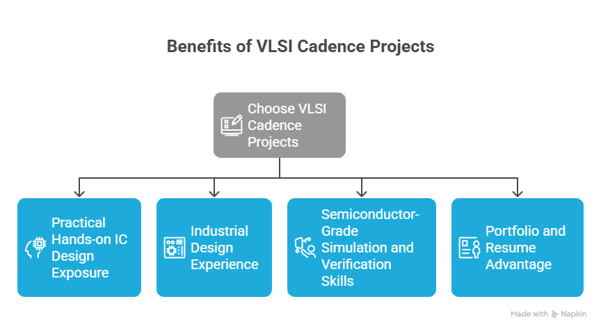
✔ Practical hands-on IC design exposure
✔ Industrial design experience
✔ Semiconductor-grade simulation and verification skills
✔ Portfolio and resume advantage for core engineering jobs
FAQ
1. Is Cadence Virtuoso suitable for student-level projects?
Yes, it is widely used in academic research and industry-level chip design.
2. Do VLSI Cadence Projects require prior simulation experience?
Basic electronics and device modeling knowledge is recommended.
3. Can these projects be extended to IEEE journal publication?
Yes—each topic has strong research potential and real-world application relevance.
4. Are these projects suitable for internships and university labs?
Absolutely. Most companies value Cadence experience during VLSI hiring.
5. Can students integrate digital design into these VLSI Cadence Projects?
Yes—mixed-signal and AMS simulations allow integration with Verilog or SystemVerilog.
Conclusion
Working on VLSI Cadence Projects not only enhances technical knowledge but also builds confidence in silicon-proven IC design workflows. These topics prepare engineering students for semiconductor careers, research opportunities, and high-impact technology roles.
For students looking for ready-made VLSI Cadence Projects with reports, simulation files, and guidance, you can explore reliable academic project support available from MyProjectBazaar.