Low-Power Pulse-Triggered Flip-Flop Design Based on a Signal Feed-Through Scheme
Product Description
Low-Power Pulse-Triggered Flip-Flop Design Based on a Signal Feed-Through Scheme
Abstract—Abstract In this brief, a low-power flip-flop (FF) design featuring an
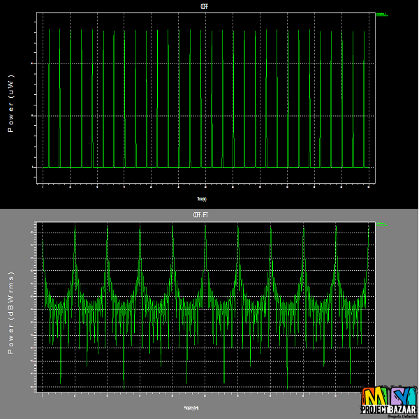
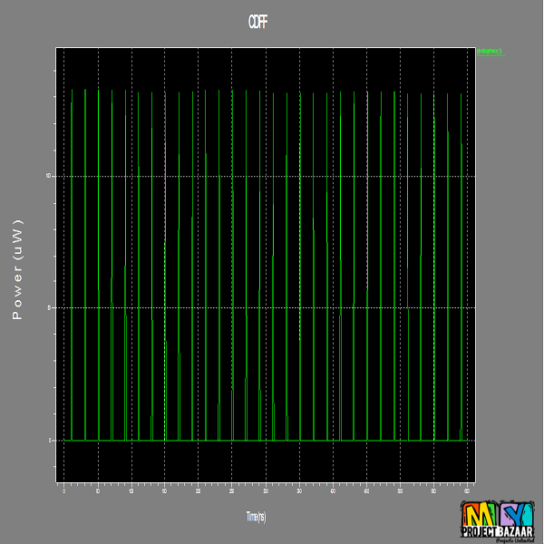
explicit type pulse-triggered structure and a modified true single phase clock latch based on a signal feed-through scheme is presented. The proposed design successfully solves the long discharging path problem in conventional explicit type pulse-triggered FF (P-FF) designs and achieves better speed and power performance. Based on post-layout simulation results using TSMC CMOS 90-nm technology, the proposed design outperforms the conventional P-FF design data-close-to-output (ep-DCO) by 8.2% in data-to-Q delay. In the mean time, the performance edges on power and power- delay-product metrics are 22.7% and 29.7% respectively.Flip-flops (FFs) are the basic storage elements used extensively in all kinds of digital designs. In particular, digital designs nowadays often adopt intensive pipelining techniques and employ many FF-rich modules such as register file, shift register, and first in first out. It is also estimated that the power consumption of the clock system, which consists of clock distribution networks and storage elements, is as high as 50% of the total system power.FFs thus contribute a significant portion of the chip area and power consumption to the overall system design.
Including Packages
Our Specialization
Support Service
Statistical Report

satisfied customers
3,589
Freelance projects
983
sales on Site
11,021
developers
175+


