Achieving Optimal Efficiency in Energy Transfer to a CMOS Fully Integrated Wireless Power Receiver
Product Description
Achieving Optimal Efficiency in Energy Transfer to a CMOS Fully Integrated Wireless Power Receiver
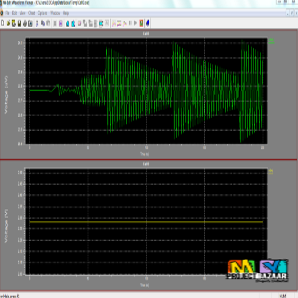
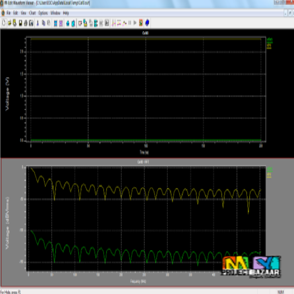
Abstract— The design and measurement of an inductive link for transferring energy to a fully integrated wireless power receiver. The power receiver design was focused on optimizing each factor that contributes to the link efficiency while its size was constrained to 1.5 mm × 1.5 mm in a conventional CMOS 180-nm process. On the power transmitter side, the primary inductor is printed on an FR4 board and its dimensions are selected so as to optimize its quality factor and the magnetic coupling factor. A strategy is proposed to experimentally determine the erformance of the entire system. Using the proposed strategy, we measured a link efficiency of −25.4 dB at a frequency of 986 MHz, with a primary inductor of average diameter 22 mm and distance 15 mm from the receiver. Considering the characteristics of the receiver: monolithic implementation, chip area, link efficiency, and distance to the transmitter, the designed wireless power transfer system exhibits a better performance than state-of-the-art systems. Energy harvesting from the surroundings or wireless power transfer (WPT) are candidates to replace energy carriers in min iaturized circuits. This paper reports measurements obtained on a WPT system including a fully integrated CMOS batteryless receiver. < final year projects >
Including Packages
Our Specialization
Support Service
Statistical Report

satisfied customers
3,589
Freelance projects
983
sales on Site
11,021
developers
175+


